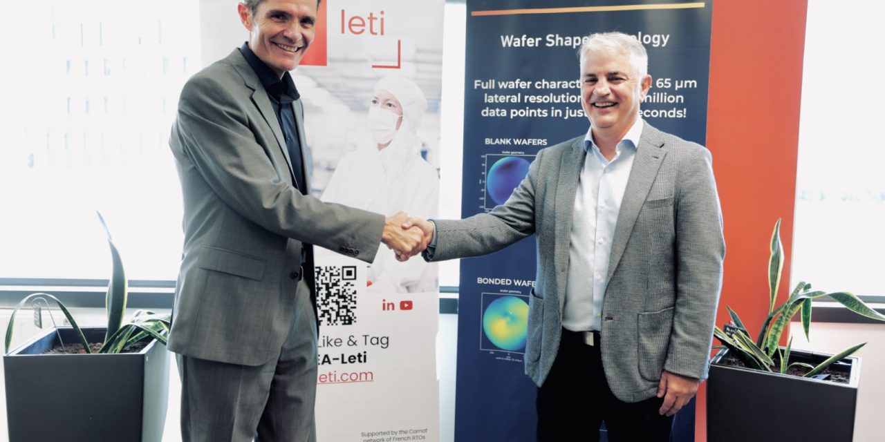
Wooptix, an innovation leader in semiconductor wavefront phase imaging metrology, has announced the installation of its Phemet system at CEA-Leti’s Grenoble technology research institute, marking a significant milestone in the company’s expansion into semiconductor metrology and process control.
Installed on May 4, 2026, the system will support joint work on wafer-scale process signatures, nanotopography, and advanced packaging metrology in an industrial semiconductor cleanroom environment. The joint agreement was highlighted during CEA-Leti Innovation Days/LID World Summit, the institute’s flagship annual event that took place in June 23-25 in Grenoble.
“This installation marks a major milestone for Wooptix and a necessary step in our roadmap toward high-volume semiconductor manufacturing applications,” said José Manuel Ramos, CEO, Wooptix. “Our collaboration with CEA-Leti will allow us to validate Phemet in a highly controlled semiconductor cleanroom environment and to build application evidence around real process-development challenges alongside some of the world’s leading players. The project strengthens our presence in Grenoble, a dynamic European semiconductor hub.”
The installation is the first deployment of Wooptix’s Phemet production metrology tool. The collaboration will enable Wooptix to test and refine its technology directly in product-relevant processes while exploring new use cases within one of Europe’s most sophisticated R&D facilities.
“CEA-Leti is excited to evaluate the capabilities of the first fully automated Phemet 300 mm platform—a significant milestone that will enable the deployment of a wide range of applications at industrial scale. Our collaboration with Wooptix opens new opportunities to tackle cutting-edge challenges in nanotopographic metrology,” said Viorel Balan, Collaboration Project Manager. “By leveraging the Phemet platform, we aim to deepen our understanding of the processes, support research initiatives within European Union projects, and accelerate the development of next-generation advanced packaging technologies.”
Read other recent instrumentation news: https://instrumentation.co.uk/category/news/