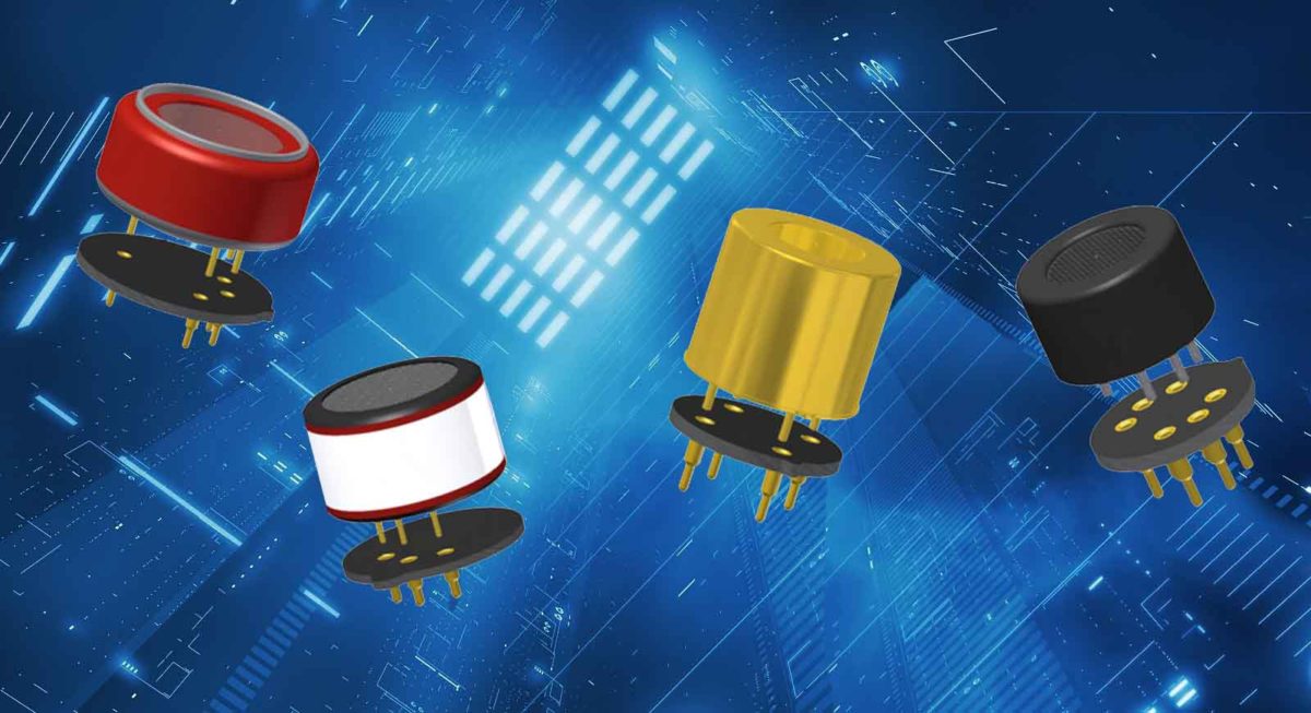
 Andon Electronics make precision sockets used in the testing and board-level assembly of image sensors, optoelectronic and gas sensors, DC-DC converters, batteries, crystal oscillators, fuses, relays, and more.
These innovative and effective components are available exclusively in the UK from Luso Electronics.
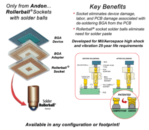
Leading OEMs and contract manufacturers solder Andon sockets – not the devices –onto the PCB.
What are the advantages of using Andon Sockets?
- Reduction in device damage from exposure to high temp solder, ESD, and cleaning solutions
- Reduction in solder joint cracking and associated intermittency
- Removal of the labour costs and PC board damage associated with de-soldering a faulty device
- Stop holding up PCB assembly until the devices arrive, build your pcbs then add the expensive components later as required, improving cashflow.
- Reduce damage caused by excessive heat and noise.
John O. Tate, Andon President, pioneered many of the innovative, high-reliability interconnects for military, aerospace and commercial applications that have become industry standards. In 1965, he developed the stamped and formed multi-finger precision socket contact, which remains the preferred method throughout the world for connecting today’s critical components.
Standard and custom sockets are available for a variety of package outlines including PGAs , BGAs , CLCCs , PLCCs , TOs , DIPs , SIPs , LEDs , and more.
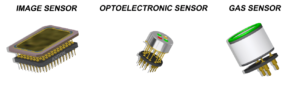
Sensor sockets
Andon Electronics provide interconnection components that help companies to cost effectively protect, assemble, test and replace their semiconductor devices.
These sockets eliminate risks associated with Electrolytes, High Temperatures and Solvents that could damage your sensors.
Solder Andon sockets on the PCB and plug-in the Sensor after all other assembly and testing. Sockets are available for all brands of sensors, with footprints that are the same as the sensor.
Benefits of using Andon sockets for your sensor application
- Complete rework and testing without the sensor, reduces risk of damage and loss.
- Enables easy field replacements and upgrades of sensors.
- Improves cash flow by volume PCB assembly cost savings; soldering Andon Sockets on to your PCB’s and then buy Sensors as needed.

Opto sockets
Customers will appreciate knowing that production line PCB assembly problems with Optoelectronic devices such as lead soldering and thermal damage are eliminated when an Andon socket is used. No need to worry about “lead free” high temperature soldering.
Reduced handling means reduced ESD problems, no cleaning solution on the device window, no humidity or extreme temperature damage.
Allows you to keep Optoelectronic & Gas Sensor devices properly stored until ready to plug-in to the Andon socket.
Some advantages to using Andon Sockets
- Eliminate ESD from handling
- Eliminate damage from high temperature soldering and PCB cleaning solvents
- Avoid cracking of glass seals
- Reduction in shock damage to wire bonds
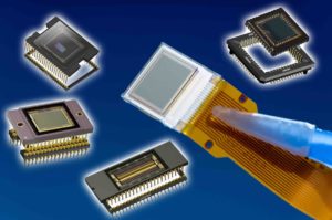
Specialist Image Sensor Sockets
Andon has developed the largest line of Image Sensor Sockets in the industry. We have sockets for Atmel, Dalsa, E2V, Fairchild, Hamamatsu, Kodak, Marconi, Micron, Motorola, National, NEC, Peripheral Imaging, Phillips, Site, Sony, TI, and Toshiba.
Image Sensor sockets provide higher reliability because the sockets can be soldered to the motherboard in large quantities. Later, as required, the sensors can be plugged-in or unplugged and upgraded easily.
Advantages of using sockets with Image Sensors
- Reduce static discharge (ESD) because of less handling.
- Eliminate soldering temperature which can affect the colour array.
- Eliminate need to de-solder CCD.
- Eliminate cleaning solution, scratches to glass plate, and risk blistering the PCB.
- Eliminate assembly line temperatures, humidity, and shock.
LCC Image Sensor sockets
These sockets with their unique design avoid cracking of solder joints and ceramic substrate:
LCC Image Sensors are packaged with up to 100 castellations (contacts). The ceramic substrate packaging presents new challenges for RoHS high temperature soldering. Utilisation of Andon’s unique LCC sockets eliminating the cracking of LCC Substrate and Solder Joints. Historically, Image Sensors are soldered directly on the printed circuit board (PCB). LCC Image Sensors require longer soldering times for RoHS high temperature solders. The ceramic substrate “expands” while the solder joint is “fixed” and cracks.
So, utilisation of Andon sockets can simplify the production process, reduce cash flow, decrease costs, improve yields and eliminate causes of device damage with improved handling.
Please contact Luso to discuss your application and assistance with selection of the right socket for your design.
Luso are exhibiting at Sensors & Instrumentation Live this September at the NEC, 29/30 September. Instrumentation Live
