Features

Anritsu and Bluetest supporting OTA measurements on IEEE 802.11be (Wi-Fi 7) devices

Anritsu and Bluetest combine their recent product upgrades to create an Over-the-Air (OTA) measurement solution for verifying RF performance in tri-frequency bands of the latest WLAN standard (IEEE 802.11be). This collaboration provides customers with a WLAN test solution capable of transmit power (TRP) and receive sensitivity (TIS) measurements on IEEE 802.11be supported devices. Measuring the OTA performance in life-like, but repeatable conditions, enables manufacturers of high-speed data transmission devices, including high-end smartphones, AR/VR devices and cloud gaming consoles, to optimize the radio performance and end-user satisfaction.

IEEE 802.11be is being standardized as the successor to IEEE 802.11ax (Wi-Fi 6/6E) and is targeted to realize high-speed communications that significantly exceed IEEE 802.11ax. The standard is expected to be a fundamental technology supporting the latest applications and services, such as ultra-high resolution video streaming beyond 4K and AR/VR.

Although the official release of the standard is scheduled for 2024, product development based on the draft standard is underway, and leading companies have already begun to bring their products to market. IEEE 802.11be adopts innovative technologies such as 320 MHz bandwidth, 4096 QAM modulation and Multiple RU, and a comprehensive evaluation of RF performance is required.

The Anritsu Wireless Connectivity Test Set MT8862A is dedicated to the WLAN standard, hence optimized for stable and reliable connections with wider dynamic range, even in a faded environment such as in the Bluetest reverberation chamber. It is now updated with a new radio module adding support for 320 MHz bandwidth, in addition to the supported 2.4, 5 and 6 GHz bands. The test setup is easily expanded to support 2×2 MIMO measurements using two MT8862A units.

Bluetest Product Manager Klas Arvidsson says: “The combination of Bluetest reverberation chamber test system and Anritsu MT8862A offers a compact and fast solution for evaluating WLAN device performance. Various sizes of chambers, from the very compact, “fits-through-an-office-door”, RTS25 up to the walk-in RTS95 chamber, caters for measurements on small, as well as very large WLAN devices such as television screens or other home appliances. It is even possible to measure wearables while used by a real person.”

Keita Masuhara, Product Manager, IoT Test Solutions Div., Anritsu Corporation, adds: “IEEE 802.11be is not only an extension of the physical layer technology, but also adopts innovative technologies such as Multi-link Operation, which enables easier comfortable high-speed communication than ever before by efficiently using three frequency bands simultaneously. However, specific performance evaluation is necessary to prevent problems and realize its full potential. Anritsu has worked with Bluetest to provide a valuable solution for OTA RF performance evaluation. We are confident that the new measurement system will contribute to efficient performance testing.”

The Anritsu MT8862A and all Bluetest chambers are available for order, and upgrade packages are offered for already installed systems.

CommScope and STMicroelectronics make Matter provisioning for IoT devices secure and easy

CommScope, a global leader in network connectivity,  and STMicroelectronics, a global semiconductor leader serving customers across the spectrum of electronics applications, announced today the integration of CommScope’s PKIWorks IoT security platform with ST’s popular STM32WB microcontroller unit (MCU). This integrated solution offers device manufacturers a turnkey solution for developing IoT devices that meet the Connectivity Standards Alliance Matter standard for security.

The solution simplifies manufacturing secure Matter-device-credentials development and provisioning, in addition to reducing costs and time for IoT device manufacturers. With this integration, devices can be commissioned at the MCU level without developer intervention. This collaboration harnesses 35 years of experience from the CommScope Sentry team securely integrating cryptographic keys and digital certificates into high-volume manufacturing production with ST’s leadership in microcontrollers and development ecosystem.

“As a CSA promoter, ST is committed to making Matter development seamless for all device makers,” said Nathalie Vallespin, STM32 Connectivity product line manager, STMicroelectronics. “Our #1 ranking for general-purpose microcontrollers and expertise in secure elements positions us to combine our deep understanding of device-makers’ challenges and strong knowledge of Matter to create unique collaborations like this one with CommScope. This will accelerate the adoption of Matter development through an easy and secure process for credential provisioning.”

“By integrating the CommScope Sentry PKIWorks platform with ST’s popular MCU platform, we’re offering our customers a turnkey solution to alleviate the challenges of Matter adoption, while handling the complexity, scale, and cost,” stated Bart Giordano, president, Networking, Intelligent Cellular and Security Solutions, CommScope. “CommScope and ST have a long-standing collaborative relationship, making it easy to meet growing demand for new Matter IoT devices with the expertise of two industry leaders with decades of experience at the forefront of digital security, semiconductor solutions, and device manufacturing.”

Anritsu enhances WLAN tester to support Wi-Fi 7 with network mode

With the launch of devices based on the new Wi-Fi 7 communications standard, there is already a growing demand for test instrumentation that can evaluate them.

To meet this need, Anritsu Corporation introduces a new Network Mode option for its MT8862A Wireless Connectivity Test Set, allowing the instrument to evaluate the Wi-Fi 7 signal quality of devices under test.

Developed by the Institute of Electrical and Electronics Engineers, the IEEE802.11be (Wi-Fi 7) wireless communication standard is the successor to the IEEE802.11ax (Wi-Fi 6/6E) WLAN standard. The new standard is designed to achieve a transmission speed of 30 Gbps or more, much faster than Wi-Fi 6/6E. In addition to extending conventional technologies, including 4096 QAM, 320 MHz channel bandwidth, and Multi-RU, Wi-Fi 7 also adopts new technologies such as Multi-Link Operation (MLO), enabling a device to simultaneously send and receive data across different frequency bands and channels.

With the new Network Mode option, Anritsu is playing a major role in improving the signal quality of Wi-Fi 7 devices and contributing to the growth and success of this important new communications protocol.

Development Background

The development of the Wi-Fi 7 standard is scheduled for completion in 2024 and is expected to be used for devices that support the latest applications and services, such as ultra-high-definition video streaming and AR/VR. Devices using chips based on the draft standard of Wi-Fi 7 have already appeared and there is rapidly increasing demand for test instruments to evaluate these devices.

Product Summary and Features

  • Wi-Fi 7 RF Evaluation Capability with Network Mode

Because the signal quality of WLAN varies with the data rate, it is very important to evaluate the signal at each of the proposed rates. The MT8862A allows the user to specify the data rate for the test, enabling RF evaluation to be conducted at all the data rates used by the major WLAN standards, including Wi-Fi 7.

  • Flexible Test Environment

Provides a test environment for evaluating RF TRX characteristics (TX power, modulation accuracy, RX sensitivity, etc.) of WLAN devices, including Wi-Fi 7.

Click to learn more about MT8862A.

PowTechnology’s IIoT solution helps Green Biofuels convert customers to environmentally friendly HVO fuel

PowTechnology is delighted to share its latest case study.

The Task

Green Biofuels is the UK’s leading provider of Hydrotreated Vegetable Oil fossil free diesel replacement (HVO). They distribute a million litres/day. Trial tanks are provided to potential users. Remote monitoring was needed to ensure continuous availability of HVO to assist trial success on construction sites with no power infrastructure.

The Solution 

PowTechnology’s battery-powered Metron4 telemetry devices are now installed on all trial tanks. Full technical support and training was provided. Regular tank level data and low level alerts are displayed via PowTechnology’s versatile  MetronView IoT platform, visible on any web-enabled device. Data enables centralised logistics to schedule efficient, cost-effective deliveries.

The Result

This PowTechnology digital transformation solution has ensured that no trial site has run-out of HVO, resulting in successful trials and a near complete conversion rate. HVO achieves an 80-90% cut in harmful emissions, which is great news for the environment and Green Biofuels benefit from efficient logistics and new customers. 

Summary

  • Simple retrofit
  • Increased trial success
  • Business growth
  • Reduced logistics costs
  • Environmental benefits

Pete Moore, Lead Engineer, Green Biofuels comments: “PowTechnology’s IIoT solution has done everything we asked for. Data is reliable and we no longer suffer from regular run outs. The initial technical support and training was ideal and we are now self-sufficient. We are delighted that so many trials are turning into regular business and we have no hesitation in recommending PowTechnology to others.”

> > Download Case Study

PowTechnology offers over 30 years’ experience in instrumentation, communications and software, delivering remote monitoring solutions globally, across a broad range of industries and applications.

The company provides digital transformation solutions, integrating its own innovative IIoT hardware and software with trusted third-party instrumentation and technologies, which can be customised to meet specific needs.

PowTechnology solutions deliver data from sensors and machines to the cloud, improving reliability, performance and sustainability.

The company works with its customers to help them lower operational and energy costs, prevent breakdown, maximise resource, comply with legislation, introduce new revenue streams, improve service and differentiate themselves from competitors. 

The modular, highly scalable design of our IIoT solutions allow us to develop versatile digital transformation ‘building blocks’ which enable the speedy development of custom solutions.

Whether you need robust, proven, off-the-shelf Industry4.0 kit or a tailored, application-specific development, PowTechnology solutions are fit to purpose, with controlled whole of life project costs and comprehensive technical support.

PowTechnology is ISO9001 and ISO27001 accredited.

To see over 30 PowTechnology case studies, please click here:

Please browse PowTechnology’s web site and get in touch with any queries or applications you would like to discuss.

How can PowTechnology help you?

+44 1827 310 666 sales@PowTechnology.com or use this contact form.


Farnell introduces expanded interconnect solutions from premium manufacturers

Farnell a fast and reliable distributor of products and technology for electronic and industrial system design, maintenance and repair has announced a significant expansion of its interconnect product portfolio.

This strategic initiative introduces an impressive selection of high-quality interconnect solutions from industry leaders, providing customers with a broader spectrum of cutting-edge products. Notable brands, including TE Connectivity, Molex, Amphenol, Harting, Phoenix Contact, Anderson Power Products, Aptiv, and Alpha Wire, have contributed to this extensive range.

The expanded interconnect range encompasses a diverse selection of products, from connectors to cables, designed to address a wide range of applications. Key features of these interconnect products include industry-leading quality, reliability, and performance, ensuring seamless connectivity, enhanced durability, and compatibility across various industries, including electronics manufacturing, automotive, telecommunications, aerospace, and renewable energy.

Russell Paik, Interconnect Product Manager at Farnell stated, “As our customers continue to push the boundaries of innovation, we at Farnell are driven by an unwavering commitment to expand our offerings. Our goal is to not just meet but exceed their expectations, and this expansion is a testament to our dedication in becoming the go-to brand for bringing their boldest innovations to life.”

Customers across the Asia-Pacific, Europe, Middle East, and Africa (EMEA), and North America (NA) regions can explore the expanded interconnect range by visiting dedicated online platforms on element14, Newark, and Farnell

Fluke enables engineers to prioritise arc flash safety with range of thermal imaging and wireless testing tools

Fluke, a global technology leader in the manufacture of compact, professional electronic test and measurement tools and software, has developed a range of thermal imaging and wireless testing tools designed to ensure safety is the top priority for engineers working in potentially dangerous arc flash zones.

Every company’s electrical safety strategy should be based around limiting workers’ exposure to such electrical hazards as arc flash and electrocution. Fluke says the best way to keep operators out of harm’s way is to give them access to the right non-contact tools that not only protect them but also reduce dramatically (by up to half) the amount of time they are required to work on live circuits in arc flash zones.

Arc flash is the light and heat created from an arc fault explosion and temperatures can reach up to 19,000°C (35,000°F), capable of igniting an operator’s clothing and burning the skin of anyone within a few feet. Arc flash can also melt metal, cause lung and eyesight damage and lead to hospitalisation, even death.

Engineers and health & safety teams will be familiar with the need to establish arc flash boundaries and wear arc-rated clothing and rubber insulating gloves. However, using non-contact test and measurement tools means operators are able to minimise the level of personal protective equipment (PPE) required as well as the amount of time they need to spend inside the boundary.

One such product is Fluke’s PQ400 electrical measurement window (EMW), which is permanently installed into cabinets with voltage and current connections made inside the panel. The PQ400 gives workers access to critical power quality and energy data while decreasing testing time and maintaining a high level of safety. Users can plug their power quality tools directly into the EMW to collect all the data that’s needed.

As well as the safety aspects, advantages of using the PQ400 include lower maintenance costs and reduced downtime by being able to make critical power quality and energy measurements without opening the panel door. The EMW also enables logging and monitoring to be done at any time, without disrupting operations, while measurement efficiency is increased.

A second product – Fluke’s CV400 ClirVu 4in window – is a permanent infra-red window that provides a view of what’s on the other side of a panel without workers being exposed to live voltage or needing full PPE. Offering the most visibility into a panel for a thermal camera (simplifying the inspection process by allowing measurements to be taken without having to open a cabinet), the widest Fluke window option available also helps to reduce time and costs involved in preventive maintenance.

Likewise, Fluke’s TiS75+ thermal camera enables operators to capture and measure heat energy emanating from a source without having to make physical contact, meaning they can see instantly what’s running too hot or too cold before anything breaks down. Offering one-handed image capture, review and save facilities, the camera not only helps operators to keep a safe distance from an arc flash boundary but also allows them to compare thermal scans over time using the Fluke Connect app.

A fourth product – the Fluke 376 FC clamp meter – makes it possible to set up measurements and transmit the data from inside the arc flash boundary, meaning someone within 20m of the equipment is able to open the Fluke Connect app and read the figures from outside the boundary. As well as reducing the time technicians spend in the arc flash boundary, the clamp meter helps them to log, trend and monitor measurements remotely so they can pinpoint intermittent faults.

Finally, the Fluke 3000FC digital multimeter is a flexible DMM allowing users to read results through the Fluke Connect app, outside the arc flash boundary. Using this equipment cuts the time technicians spend inside the boundary and offers them an easy-to-read display with large digits and bright backlight.

Says Eric van Riet: “There’s no need for engineers to put themselves in an arc blast zone if they can avoid being there. Products such as wireless and non-contact tools as well as remote displays can help place them as far away as possible from risk and danger while allowing them to take accurate, instant readings that can be analysed remotely. Arc flash safety is essential, and the latest thermal imaging and wireless testing tools are the best way to offer operators maximum protection.”

For more information, visit www.fluke.com.

New eBook from Mouser Electronics and NXP Semiconductors offers insights into design challenges for vehicle electrification

Mouser Electronics, Inc., the industry’s leading New Product Introduction (NPI) distributor with the widest selection of semiconductors and electronic components™, launched a new eBook in collaboration with NXP Semiconductors, a world leader in secure connectivity solutions for embedded applications, which is pushing boundaries in the automotive, industrial and IoT, mobile, and communication infrastructure markets while delivering solutions that advance a more sustainable future. In this eBook, Mouser and NXP explore design challenges in vehicle electrification systems, with insights into potential pathways for solutions.

In 7 Experts on Designing Vehicle Electrification Solutions, the new eBook from Mouser and NXP, subject matter experts from across the electric vehicle (EV) industry and NXP offer their perspectives on how they’re addressing challenges surrounding data-driven optimization, safety, EV charging and efficiency, to help manufacturers bring innovation to the EV market in record time. Modern EVs, with advanced driver assistance systems, feature dozens of integrated sensor systems that work together to achieve higher performance and enhance driver safety. These sensors also gather actionable data regarding the EVs subsystems, including motor and battery performance, and most importantly, provide a wealth of data-driven information to facilitate system optimization while refining EV design decisions into the future.

The eBook explores how NXP and Mouser deliver data-driven technology solutions to the EV market’s specific challenges, like charging compatibility, battery lifespan, capacity, navigation and safety, and emerging innovations to improve EV efficiency and design. Of course, safety is the paramount consideration in vehicle electrification design. NXP provides a suite of analog sensing hardware solutions to help obtain vehicle data and offers a variety of low-power, scalable, functional, and safe microcontrollers for streamlining secure communications and improving performance.

7 Experts on Designing Vehicle Electrification Solutions includes product information on the latest related NXP solutions, available at Mouser Electronics, like NXP’s S32K3 microcontrollers, a family of scalable 32-bit Arm® Cortex® -M7 based MCUs in single, dual and Lockstep core configurations supporting up to ASIL D level safety. Also featured are NXP’s GD316x family of ASIL D compliant, high voltage isolated gate drivers, that offer efficiency-enhancing features such as dynamic gate strength control and segmented drive. The advanced, functionally safe HV gate drivers GD3162 and GD3160 provide a high level of integration, allowing for a smaller footprint and simplified design for xEV traction inverters.

To learn more about NXP products available from Mouser, visit https://www.mouser.com/manufacturer/nxp-semiconductors/.

To read the new e-book, visit https://resources.mouser.com/manufacturer-ebooks/nxp-7-experts-on-designing-vehicle-electrification-solutions/.

To browse all of Mouser’s eBooks, visit https://resources.mouser.com/manufacturer-ebooks/.

MEMS veteran, Matt Crowley, joins Nanusens as strategic advisor

Nanusens has announced that Matt Crowley has joined the company as a strategic advisor.

Nanusens CEO, Josep Montanyà, said, “A veteran of the MEMS industry, having worked on MEMS and sensors at Sand 9, Vesper and Qualcomm, Matt’s experience will be invaluable in helping Nanusens rapidly bring its MEMS-within-ASICs™ technology to market.”

Matt Crowley said, “The fabless semiconductor industry has thrived for decades because it uses a single standard manufacturing process, CMOS, that allows the industry to achieve massive scale, lower cost and constantly improving performance. This dynamic does not exist in the MEMS industry which is why it takes many years and tens of millions of dollars to create a new MEMS product. Nanusens is the first MEMS company to convincingly demonstrate technology that will change this paradigm by making MEMS directly in CMOS itself.

“When I first met Nanusens’ CEO, Josep Montanyà, I was sceptical of his claim that Nanusens can make a variety of MEMS devices such as accelerometers, pressure sensors and antenna switches. As someone with 20 years of experience in MEMS, I have seen many claims that could not live up to the hype, but, as I dug into the data and asked hard questions, I became convinced that, although it has not yet been proven at scale, this technology does work. Transforming the MEMS business model from one with discrete devices manufactured on dedicated lines to MEMS as a licensable IP block at major CMOS foundries will change the paradigm for a wide class of MEMS devices. It is a bold vision and I am thrilled to join Nanusens as an advisor to help make that vision a reality.”

Technology backgrounder

Nanusens is the only company to have perfected the building of sensors within chips. The sensors, called MEMS, are built using the standard chip manufacturing techniques, called CMOS, that are used to build the electronic circuits on chips and at the same time as the rest of the chip circuitry. This means that chips with Nanusens embedded sensors can be made in any of the many CMOS fab in virtually unlimited numbers and with the high yields that are normal in such fabs with all the benefits of low unit costs that fab production provides.

A key new innovation by the company is development of a novel control circuit that measures the capacitance changes within the sensor to provide sensor data. Like the sensor itself, this is also a digital IP block so it can be incorporated in the floor plan of the device’s control chip, or ASIC, using standard EDA tools. This pairing for sensors and control circuitry as IP is unique as no other sensor solution can be turned into an IP block and made using standard CMOS techniques within the layers of the chip structure. This also significantly reduces the complexity and bill of materials costs for an AIoT device.

Nanusens has already built accelerometer sensors into an ASIC chip using this unique technology. It is developing many other different types of embedded sensors such as gyroscope, magnetometer, pressure sensor, microphone, IR imagers and gas sensor as most of these are variants on the accelerometer design. These open up many other massive markets for its embedded sensors such as smartphones, earbuds, wearables, automotive, medical equipment and aerospace, to name but a few. As a result, the company has started a Series A funding round.

Further details of Nanusens MEMS-within-ASIC™ technology can be found at www.nanusens.com

New at Mouser: The TDK InvenSense ICU-20201 Time-of-Flight Range Sensor

Mouser Electronics, Inc., the authorized global distributor with the newest electronic components and industrial automation products, is now shipping the ICU-20201 Time-of-Flight (ToF) range sensor from TDK InvenSense. The ICU-20201 is a miniature, ultra-low power (1.8 V), long-range ultrasonic sensor based on patented compressed high-intensity radar pulse MEMS technology, ideal for smart door lock wake-on-approach, wall following, obstacle avoidance, parking lot sensors for vehicle counting, and ground-level measurement in drones.

The TDK InvenSense ICU-20201 ToF range sensor, available from Mouser, offers multi-object detection and accurate range measurements to targets up to 5 meters and can operate in any lighting condition, including full sunlight to complete darkness. Featuring an integrated 85 kHz piezoelectric, micromachined ultrasonic transducer (PMUT) with a 2nd generation ultra-low power System on Chip (SoC), this reflowable package also offers a customizable field-of-view (FOV) up to 180° and a single sound port for receiving and transmitting.

The ICU-20201 sensor is supported by the EV_ICU-20201-00 evaluation board. The evaluation board includes the ICU-2021 ultrasonic sensor device, support circuitry, test points and a 12-pin 0.5 mm pitch flat flex cable (FFC) connector. This board requires an acoustic housing to interface with the IC.

Additionally, Mouser stocks the DK-x0201 development kit for the ICU-2021 Ultrasonic Time-of-Flight (ToF) sensor. This kit includes a development host board featuring the Microchip Technology SAMG55 microcontroller, a daughter evaluation board, and a target board with a pre-mounted ICU-2021 sensor. The kit enables rapid evaluation and development of the ICU-20201 sensor when connected to a PC running the downloadable GUI-based development software and embedded drivers.

To learn more about TDK InvenSense ICU-20201 ToF sensor, visit https://www.mouser.com/new/tdk/tdk-icu-20201-tof-sensor/.

To learn more about the EV_ICU-20201-00 evaluation board, visit https://www.mouser.com/new/tdk/tdk-ev-icu-20201-00-eval-board/.

To learn more about the DK-x0201 development kit, visit https://www.mouser.com/new/tdk/tdk-dk-x0201-dev-kit/.

K- and L-coded panel mount parts according to UL 2237: Power connectors for the North America market

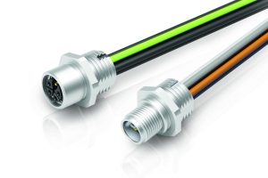
Power supply components intended for control cabinets on the North American continent must meet the specifications of the UL 2237 standard. Engineers at binder have designed panel mount parts with K and L coding as part of the M12 series 824 and 823, which comprehensively follow these requirements.

binder, a leading supplier of industrial circular connectors, offers K- and L-coded panel mount parts within its 824/823 product series, which are intended for power applications in the North American market in compliance with the UL 2237 standard. These include 5-pin male and female panel mount parts featuring screw locking that meet the protection degree criteria of IP68. Electrical and plant engineering as well as industrial controls are the main application areas for these M12 components.

UL 2237 – panel mount parts for North America

The use of electromechanical interfaces for voltage and power transmission in control cabinets of the North American applications market requires approvals according to UL 2237. This standard specifies testing guidelines for connectors, cables, cable glands, and fuse elements, such as the Grounding (Bonding) Path Current Test: this procedure stipulates the PE path (protection earth) to withstand a current of 190 A for the wire gauge AWG16 or 300 A in the case of AWG14 for four seconds without interrupting. AC applications also require an abnormal-overload test to be carried out at 1.5 times the rated current – where the PE path fuse must not blow – as well as an additional connection of the PE pin to the component housing.

Panel mount parts featuring K and L coding

According to the DIN EN 61076-2-111 standard, K coding indicates 5-pin M12 connectors for power supply to AC applications such as drives or frequency converters. The rated voltage and current limits are specified at 630 V(AC) and 12 A, respectively. The L coding also refers to a 5-pole mating face but is particularly designed for DC applications up to 63 V(DC) and 16 A. These include, for example, smaller motors or fieldbus devices in the industrial-automation sector.

824 and 823 panel mount parts at a glance

The 5-pin panel mount parts of the binder 824 and 823 series with K coding (pin count 4+PE) and with L coding (pin count 4+FE, functional earth) feature M12 screw locking. The termination types are single wires. Both the K- and L-coded components were designed for wire gauges AWG16 and AWG14. For the AC components with K coding, the requirements of UL 2237 were implemented via a PE connection to the threaded ring. UL 2237 approval is currently being prepared.

The mechanical lifespan of the panel mount parts is rated at >100 mating cycles. The temperature limits are -40/+85 °C (Series 824) and -40/+105 °C (Series 823).